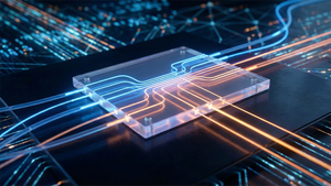
As 2025 draws to a close, the semiconductor industry is reflecting on a year of unprecedented growth, and no company has captured the market's imagination—or capital—quite like Lam Research (NASDAQ: LRCX). With a staggering 127% year-to-date surge as of December 19, 2025, the California-based equipment giant has officially transitioned from a cyclical hardware supplier to the primary architect of the AI infrastructure era. This rally, which has seen Lam Research significantly outperform its primary rival Applied Materials (NASDAQ: AMAT), marks a historic shift in how Wall Street values the "picks and shovels" of the artificial intelligence boom.
The significance of this surge lies in Lam's specialized dominance over the most critical bottlenecks in AI chip production: High Bandwidth Memory (HBM) and next-generation transistor architectures. As the industry grapples with the "memory wall"—the growing performance gap between fast processors and slower memory—Lam Research has positioned itself as the indispensable provider of the etching and deposition tools required to build the complex 3D structures that define modern AI hardware.
Engineering the 2nm Era: The Akara and Cryo Breakthroughs
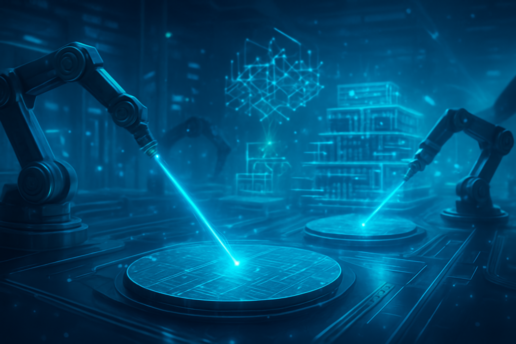
The technical backbone of Lam’s 2025 performance is a suite of revolutionary tools that have redefined precision at the atomic scale. At the forefront is the Lam Cryo 3.0, a cryogenic etching platform that operates at -80°C. This technology has become the industry standard for producing Through-Silicon Vias (TSVs) in HBM4 memory. By utilizing ultra-low temperatures, the tool achieves vertical etch profiles at 2.5 times the speed of traditional methods, a capability that has been hailed by the research community as the "holy grail" for mass-producing the dense memory stacks required for NVIDIA (NASDAQ: NVDA) and AMD (NASDAQ: AMD) accelerators.
Further driving this growth is the Akara® Conductor Etch platform, the industry’s first solid-state plasma source etcher. Introduced in early 2025, Akara provides the sub-angstrom precision necessary for shaping Gate-All-Around (GAA) transistors, which are replacing the aging FinFET architecture as the industry moves toward 2nm and 1.8nm nodes. With 100 times faster responsiveness than previous generations, Akara has allowed Lam to capture an estimated 80% market share in the sub-3nm etch segment. Additionally, the company’s introduction of ALTUS® Halo, a tool capable of mass-producing Molybdenum layers to replace Tungsten, has been described as a paradigm shift. Molybdenum reduces electrical resistance by over 50%, enabling the power-efficient scaling that is mandatory for the next generation of data center CPUs and GPUs.
A Competitive Re-Alignment in the WFE Market
Lam Research’s 127% rise has sent ripples through the Wafer Fabrication Equipment (WFE) market, forcing competitors and customers to re-evaluate their strategic positions. While Applied Materials remains a powerhouse in materials engineering, Lam’s concentrated focus on "etch-heavy" processes has given it a distinct advantage as chips become increasingly three-dimensional. In 2025, Lam’s gross margins consistently exceeded the 50% threshold for the first time in over a decade, a feat attributed to its high-value proprietary technology in the HBM and GAA sectors.
This dominance has created a symbiotic relationship with leading chipmakers like Taiwan Semiconductor Manufacturing Company (NYSE: TSM), Samsung Electronics (KRX: 005930), and SK Hynix (KRX: 000660). As these giants race to build the world’s first 1.8nm production lines, they have become increasingly dependent on Lam’s specialized tools. For startups and smaller AI labs, the high cost of this equipment has further raised the barrier to entry for custom silicon, reinforcing the dominance of established tech giants who can afford the billions in capital expenditure required to outfit a modern fab with Lam’s latest platforms.
The Silicon Renaissance and the End of the "Memory Wall"
The broader significance of Lam’s 2025 performance cannot be overstated. It signals the arrival of the "Silicon Renaissance," where the focus of AI development has shifted from software algorithms to the physical limitations of hardware. For years, the industry feared a stagnation in Moore’s Law, but Lam’s breakthroughs in 3D stacking and materials science have provided a new roadmap for growth. By solving the "memory wall" through advanced HBM4 production tools, Lam has effectively extended the runway for the entire AI industry.
However, this growth has not been without its complexities. The year 2025 also saw a significant recalibration of the global supply chain. Lam Research’s revenue exposure to China, which peaked at over 40% in previous years, began to shift as U.S. export controls tightened. This geopolitical friction has been offset by the massive influx of investment driven by the U.S. CHIPS Act. As Lam navigates these regulatory waters, its performance serves as a barometer for the broader "tech cold war," where control over semiconductor manufacturing equipment is increasingly viewed as a matter of national security.
Looking Toward 2026: The $1 Trillion Milestone
Heading into 2026, the outlook for Lam Research remains bullish, though tempered by potential cyclical normalization. Analysts at major firms like Goldman Sachs (NYSE: GS) and JPMorgan (NYSE: JPM) have set price targets ranging from $160 to $200, citing the continued "wafer intensity" of AI chips. The industry is currently on a trajectory to reach $1 trillion in total semiconductor revenue by 2030, and 2026 is expected to be a pivotal year as the first 2nm-capable fabs in the United States, including TSMC’s Arizona Fab 2 and Intel’s (NASDAQ: INTC) Ohio facilities, begin their major equipment move-in phases.
The near-term focus will be on the ramp-up of Backside Power Delivery, a new chip architecture that moves power routing to the bottom of the wafer to improve efficiency. Lam is expected to be a primary beneficiary of this transition, as it requires specialized etching steps that play directly into the company’s core strengths. Challenges remain, particularly regarding the potential for "digestion" in the NAND market if capacity overshoots demand, but the structural need for AI-optimized memory suggests that any downturn may be shallower than in previous cycles.
A Historic Year for AI Infrastructure
In summary, Lam Research’s 127% surge in 2025 is more than just a stock market success story; it is a testament to the critical role of materials science in the AI revolution. By mastering the atomic-level manipulation of silicon and new materials like Molybdenum, Lam has become the gatekeeper of the next generation of computing. The company’s ability to innovate at the physical limits of nature has allowed it to outperform the broader market and cement its place as a cornerstone of the global technology ecosystem.
As we move into 2026, investors and industry observers should watch for the continued expansion of domestic manufacturing in the U.S. and Europe, as well as the initial production yields of 1.8nm chips. While geopolitical tensions and cyclical risks persist, Lam Research has proven that in the gold rush of artificial intelligence, the most valuable players are those providing the tools to dig deeper, stack higher, and process faster than ever before.
This content is intended for informational purposes only and represents analysis of current AI developments.
TokenRing AI delivers enterprise-grade solutions for multi-agent AI workflow orchestration, AI-powered development tools, and seamless remote collaboration platforms.
For more information, visit https://www.tokenring.ai/.